Microcircuit to 555 CA 3 switching circuit. Detailed description, application and circuits for switching on the NE555 timer. Operating modes NE555
I thought for a very long time how to explain in simple human words what a transistor is. Even if I talk about the transistor very, very superficially, I have to write at least five sheets using abstruse terms.
Then it dawned on me: after all, the main goal of my review is not to give academic knowledge (please come to the university or at least to Wikipedia for it), but to teach a novice radio amateur at least to distinguish a transistor from a capacitor and a resistor in order to successfully assemble their first designs (for example, sets Master Keith).
Therefore, it is best to put it this way: transistors are radio components with three terminals, designed to amplify and convert signals. This is how they might look in real life:
This is how the transistor is indicated in the diagram:
![]()
The transistor, as we already understood, has three terminals: base (B), collector (C), emitter (E).
An input signal is usually applied to the base, an amplified signal is removed from the collector, and the emitter is the common wire of the circuit. Of course, this is a very primitive description of the principles of operation of a transistor, and in general there are a lot of nuances, but we have already agreed that I will not torment you by reading a multi-page work.
On the radio component itself, the conclusions are not marked in any way. There is no standard for pinning either. So how do you determine where the output is?
We'll have to use the reference information: for each transistor there is a so-called datasheet, or, in other words, a radio component passport. The datasheet contains all the information on the transistor: maximum allowable current and voltage, gain, pinout and much, much more. Datasheets are easiest to search on the Internet, and the basic parameters of transistors can be found in the amateur radio literature.
Interchangeability of transistors
Since a transistor has a much more complex device and more significant parameters than a resistor, capacitor or diode, it is not easy to find an acceptable replacement for the missing component. At a minimum, the transistor to be replaced must have the same type of housing and pinout (pinout). The new transistor should have the same structure: NPN or PNP. In addition, it is necessary to take into account electrical parameters: permissible currents, voltages, in some cases - cutoff frequency, etc.
Sometimes the circuit designer does this work for you, suggesting possible transistor analogs. On the Internet and in the amateur radio literature there are also reference tables with information on possible analogs of transistors.
Instead of the original (temporarily out of stock) transistors, their analogs are also sometimes invested in the Master Kit sets, and such a replacement does not impair the quality of the finished structure.
Installing the transistor on a printed circuit board
In general, for the successful assembly of the Master Kit, it is not necessary to know where the output of the transistor is. It is enough to combine the "keys" on the transistor and on the printed circuit board - and the transistor outputs will "automatically" be installed as expected.
Take a look at the picture. The transistor has a "key" - when you look at it from above, you can clearly see that the case is semicircular. The same "key" is found on the printed circuit board. For the correct installation of the transistor, it is enough to combine the "keys" on the transistor and on the printed circuit board:
![]()
A microcircuit is an almost finished device, or, figuratively speaking, an electronic semi-finished product.
The microcircuit contains an electronic circuit that performs a specific function: it can be a logic device, a level converter, a stabilizer, an amplifier. Inside a fingernail-sized chip can contain dozens (and sometimes hundreds, millions, and billions) of resistors, diodes, transistors, and capacitors.
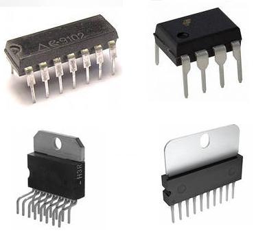
Microcircuits are available in different packages and have a different number of pins. Here are some examples of microcircuits that a novice radio amateur can work with:
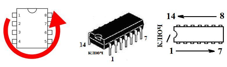
Chip pinout
Pins are numbered counterclockwise starting from the top left. The first pin is identified using a "key" - a notch on the edge of the case or a point in the form of a depression.
Interchangeability of microcircuits
A microcircuit is a highly specific ready-made electronic circuit containing a huge number of elements, and in the general case, each microcircuit is unique.
But still, in some cases, you can pick up a replacement. Different manufacturers may produce the same microcircuits. The only problem is that there is no unification in the name (sometimes, but not necessarily, the numbers of the names may coincide). For example, MA709CH, MC1709G, LM 1709L SN72710L, K153UD1A / B are the same microcircuit from different manufacturers.
In some cases, analogs of microcircuits may also be included in the Master Kit sets. This is normal and will not degrade the performance of the finished circuit.
Microcircuits - voltage stabilizers
Voltage stabilizer chips have three pins, so they can easily be confused with a transistor. But the case of this small component can contain dozens of transistors, resistors and diodes. For example, the figure below shows the 78L05 microcircuit. You can supply a voltage from 5 to 30V to its input, while the output of the microcircuit will have a constant voltage of 5V, while the load capacity of the microcircuit is 100 mA. A similar stabilizer is also available in a more powerful version - up to 1A load capacity, it is called 7805 and has a larger case.

Installing a microcircuit on a printed circuit board
There are "keys" on the microcircuit and on the printed circuit board, and when installing the microcircuit on the board, it is imperative to combine them, as shown in the figure below:

Timer NE555 is perhaps the most popular integrated circuit of its time. Despite the fact that it was developed over 40 years ago (in 1972), it is still produced by many manufacturers today. In this article, we will try to cover in detail the description and application of the NE555 timer.
Clever comparator connections, a resettable flip-flop and an inverting amplifier in a single monolithic integrated circuit, along with several other elements, have spawned the almost immortal circuitry of devices that are used by many radio amateurs today.
555 Timer was developed by the American company Signetics in 1972 and is registered in the world market. Two years later, the same company developed a microcircuit with the designation 556, which combined two separate NE555 timers with only common power pins. Even later, the 557, 558 and 559 chips were developed using up to four NE555 timers in one package. But later they were discontinued and almost forgotten.
The NE555 integrated circuit was designed as a timer and contains a combination of analog and digital elements in a single chip. It is available in various designs, ranging from the classic DIP package for standard and SOIC for SMD mounting and up to a miniature package version SSOP or SOT23-5. (NE555 Timer Prices)
The NE555 timer, in addition to the standard version, is also produced in a low-power CMOS version. The NE555's power supply is 4.5 to 15 volts (18 volts maximum), and the CMOS version uses 3 volts. The maximum output load of the NE555 output is 200mA, the low-power version of the timer only has 20mA at 9 volts.
The stability of the standard 555 is highly dependent on the quality of the power supply. It does not affect so much in simple schemes with the use of a timer, however, in more complex designs, it is advisable to install a buffer capacitor along the power circuit with a capacity of 100 microfarads.
Main characteristics of the integral timer NE555
- The maximum frequency is more than 500 kHz.
- The length of one pulse is from 1 ms to an hour.
- It can work as a monostable multi-vibrator.
- High output current (up to 200mA)
- Adjustable pulse duty cycle (the ratio of the pulse period to its duration).
- Compatible with TTL levels.
- Temperature stability 0.005% per degree Celsius.
The NE555 microcircuit contains just over 20 transistors and 10 resistors. The following figure shows a block diagram of a timer from Philips Semiconductors.

The following table lists the main properties of NE555

Purpose of terminals of timer NE555

# 2 - Start (trigger)
The flip-flop switches if the voltage at this pin drops below 1/3 of the supply voltage. This pin has a high input impedance, more than 2 mΩ. In the unstable mode, it is used to control the voltage across the timing capacitor; in the bistable mode, a switching element is connected to it, for example, a button.
No. 4 - Reset
If the voltage at this pin is below 0.7 volts, then the internal comparator is reset. In case of non-use, supply voltage must be applied to this pin of the NE555 timer. The lead resistance is about 10 kOhm.
No. 5 - Control
It can be used to adjust the output pulse duration by applying a voltage 2/3 of the supply voltage. If this pin is not used, then it is advisable to connect it to the minus of the power supply through a 0.01 μF capacitor.
No. 6 - Stop (comparator)
Stops the timer if the voltage on this pin is higher than 2/3 of the supply voltage. The pin has a high input impedance, more than 10 mΩ. It is commonly used to measure the voltage across a timing capacitor.
No. 7 - Discharge
The pin through the internal transistor is connected to ground when the internal flip-flop is active. The lead (open collector) is mainly used to discharge the timing capacitor.
# 3 - Exit
The NE555 microcircuit has only one output with a current of up to 200 mA. This is significantly more than conventional integrated circuits. The output is capable of driving, for example, LEDs (with a current limiting resistor), small light bulbs, a piezoelectric converter, a speaker (with a capacitor), an electromagnetic relay (with a protective diode) or even low-power motors direct current... If a higher output current is required, a suitable transistor can be connected as an amplifier.
Timer NE555 - wiring diagram
The ability of pin 3 of the NE555 timer to create both a high voltage level and a low (almost 0 volt) level allows you to control the load connected to both power supply minus and plus. As an example, connecting LEDs. This, of course, is not a requirement, and the load (LED) can be connected to either negative or positive of the power supply.

If the NE555 timer operates in an unstable state (generator mode), then a speaker can be connected to its output. It is connected after the blocking capacitor (for example, 100 μF) and must have a resistance of at least 64 Ohm due to the limited maximum load current of the timer output. The capacitor is designed to separate the DC component of the signal and only conducts the audio signal.

A speaker with a coil impedance lower than 64 ohms can be connected either through a capacitor with a lower capacitance (reactance), which is an additional impedance, or using an amplifier. The amplifier can also be used to connect a more powerful speaker.

Like all integrated circuits, the NE555 timer output that controls an inductive load (relay) must be protected from overvoltage surges created at the time of shutdown. A diode (e.g. 1N4148) is always connected in parallel to the relay coil in the opposite direction.

However, the NE555 requires a second diode in series with the relay coil. It limits the low voltage that is at output 3 of the timer and prevents the relay from being energized by a small current.
Such a diode can be, for example, a 1N4001 (1N4148 diode is not suitable) or an LED.
(downloaded: 3 774)
Good day, dear radio amateurs!
Welcome to the site ““
Microcircuits
Chip (IC - Integrated Circuit, IC - Integrated Circuit, chip or microchip from English Chip, Microchip) is a whole device containing transistors, diodes, resistors and other active and passive elements, the total number of which can reach several tens, hundreds, thousands, tens of thousands and more. There are many types of microcircuits. The most used among them - brain teaser, operational amplifiers, specialized.
Most of the microcircuits are housed in a rectangular plastic case with flexible plate leads (see Fig. 1) located along both sides of the case. There is a conventional key on the top of the case - a round or other shape mark, from which the pins are numbered. If you look at the microcircuit from above, then you need to count the conclusions counterclockwise, and if from below, then in the clockwise direction. Microcircuits can have any number of pins.
In domestic electronics (however, in foreign ones too), they are especially popular among microcircuits. brain teaser, built on the basis of bipolar transistors and resistors. They are also called TTL microcircuits (TTL - Transistor-Transistor Logic)... The name transistor-transistor originated from the fact that transistors are used both to perform logic functions and to amplify the output signal. Their whole principle of operation is built on two conditional levels: low or high, or, which is equivalent, the state of logical 0 or logical 1. Thus, for K155 series microcircuits, voltages from 0 to 0.4 are taken as a low level corresponding to logical 0. V, that is, not more than 0.4 V, and for a high one corresponding to a logical 1 - not less than 2.4 V and not more than a power supply voltage - 5 V, and for K176 series microcircuits, designed for power supply from a source, a voltage of 9 B, respectively 0.02. .0.05 and 8.6. .8.8 V.
Marking of foreign TTL microcircuits begins with numbers 74, for example 7400. Symbols of the main elements of logic microcircuits are shown in Fig. 2. There are also truth tables that give an idea of \u200b\u200bthe logic of the action of these elements.

The symbol of the logical element AND is the "&" (conjunction "and" in english language) inside the rectangle (see Fig. 2). Left - two (or more) input pins, right - one output pin. The logic of this element is as follows: a high-level voltage at the output will appear only when signals of the same level are at all its inputs. The same conclusion can be made by looking at the truth table characterizing the electrical state of the AND element and the logical connection between its output and input signals. So, for example, in order for the output (Out) of the element to have a high level voltage, which corresponds to the unit (1) state of the element, both inputs (In. 1 and In. 2) must have voltages of the same level. In all other cases, the element will be in a zero (0) state, that is, a low level voltage will act on its output.
Conditional logical element symbol OR - digit 1
in a rectangle. It, like the AND element, can have two or more inputs. The output signal corresponding to a high level (logic 1) appears when a signal of the same level is applied to input 1 or to input 2, or simultaneously to all inputs. Check these logical relationships of the output and input signals of this element against its truth table.
Conditional element symbol NOT - also a number 1
inside the rectangle. But it has one entrance and one exit. The small circle, which begins the communication line of the output signal, symbolizes the logical negation "NOT" at the output of the element. In the language of digital technology, "NOT" means that the element is NOT an inverter, that is, an electronic "brick", the output signal of which is opposite to the input signal in terms of level. In other words: as long as a low level signal is present at its input, it will output a high level signal, and vice versa. This is indicated by the logical levels in the truth table of the operation of this element.
Logical element NAND NOT is a combination of elements AND and NOT, therefore on its conventional graphic designation there is a sign “ &
”And a small circle on the output signal line, symbolizing logical negation. There is one exit, and two or more entrances. The logic of the element is as follows: a high-level signal at the output appears only when there are low-level signals at all inputs. If at least one of the inputs has a low-level signal, the output of the AND-NOT element will have a high-level signal, that is, it will be in a single state, and if there is a high-level signal at all inputs, it will be in a zero state. An NAND element can perform the function of a NOT element, that is, become an inverter. To do this, you just need to connect all its inputs together. Then, when a low-level signal is applied to such a combined input, the output of the element will be a high-level signal, and vice versa. This property of the NAND element is very widely used in digital technology.
The designation of symbols of logic elements (signs "&" or "1") is used only in domestic circuitry.
TTL microcircuits provide the construction of a wide variety of digital devices operating at frequencies up to 80 MHz, but their significant drawback is high power consumption.
In some cases, when high performance is not needed, but minimum power consumption is required, CMOS microcircuits are used, which are used field-effect transistors, not bipolar. Abbreviation CMOS (CMOS Complementary Metal-Oxide Semiconductor) stands for Complementary Metal Oxide Semiconductor. The main feature of CMOS microcircuits is negligible current consumption in static mode - 0.1 ... 100 μA. When operating at the maximum operating frequency, the power consumption increases and approaches the power consumption of the least powerful TTL microcircuits. CMOS microcircuits include such well-known series as K176, K561, KR1561 and 564.
In the class analog microcircuits allocate microcircuits with linear characteristics - linear microcircuitswhich include OU – Operational Amplifiers... Name “ operational amplifier”Due to the fact that, first of all, such amplifiers have been used to perform operations of summing signals, differentiating them, integrating, inverting, etc. Analog microcircuits are produced, as a rule, functionally unfinished, which opens up a wide scope for amateur radio creativity.

Operational amplifiers have two inputs - inverting and non-inverting. In the diagram, they are indicated by a minus and a plus, respectively (see Fig. 3). Applying a signal to the plus input - the output is a constant, but amplified signal. By feeding it to the minus input, an inverted but also amplified signal is obtained at the output.
In the production of radio-electronic products the use of multifunctional specialized microcircuits that require a minimum number of external components can significantly reduce the development time of the final device and production costs. This category of microcircuits includes chips that are designed for something specific. For example, there are microcircuits for power amplifiers, stereo receivers, and various decoders. They can all have a completely different look. If one of these microcircuits has a metal part with a hole, this means that it must be screwed to
radiator.
It is much more pleasant to deal with specialized microcircuits than with a mass of transistors and resistors. If earlier many parts were needed to assemble a radio receiver, now you can get by with one microcircuit.
One of the main purposes of microcontrollers is to control relatively simple devices and systems, which obviously requires polling sensors and issuing control signals to actuators. Often, the available microcontroller ports for such purposes may not be enough. One of the ways to increase the number of connected external devices can serve as shift register SN74HC595N. This microcircuit was purchased on Ru.aliexpress.com at $ 0.6 per batch of 10 pieces.
It allows using three ports of the microcontroller to control 8 outputs, which is important, this register allows a cascade connection, thus obtaining 16 or more digital outputs controlled by the same three ports of the microcontroller. Structurally, this is a microcircuit in a DIP-16 package

The microcircuit has 16 pins, which have the following purpose: Vcc and GND + 5V supply and common bus, respectively. DS is an input for data, SHcp is a synchronization input for writing the state of DS to the register memory, STcp is a control signal, at a low level of which, data from the register memory goes to the information outputs Q0-Q7, Q7 'is an output for transferring data to the next register (necessary when several registers work together), - control of enabling / disabling the outputs Q0-Q7, - zeroing the register.


For example, you can take the code from the manufacturers of the Arduino hardware platform that illustrates the operation of this register. This program sequentially outputs to the outputs Q0-Q7 a binary number from 00000000 to 11111111. For example, only five LEDs are connected, but in general it is clear that this program is just a counter from 0 to 255.
Video
As a result, we have a simple and cheap way increasing the number, but you have to pay for this with their lower speed. However, for information output devices, such as seven-segment indicators and linear LED scales, this is not very critical, since the speed of information output will still be greater than the speed of its perception by the human senses ...
Chip ULN2003 (ULN2003a)is essentially a set of powerful composite keys for use in inductive load circuits. It can be applied to control a load of significant power, including electromagnetic relays, DC motors, solenoid valves, in various control circuits, and others.
Chip ULN2003 - description
Brief description of ULN2003a. Chip ULN2003a is a Darlington transistor assembly with output keys increased power, which has protective diodes at the outputs, which are designed to protect control electrical circuits from a reverse voltage surge from an inductive load.
Each channel (Darlington pair) in ULN2003 is rated for 500mA load and can handle a maximum current of 600mA. The inputs and outputs are located opposite each other in the microcircuit case, which greatly facilitates the PCB layout.
ULN2003 belongs to the ULN200X family of microcircuits. Different versions of this IC are designed for specific logic. In particular, the ULN2003 microcircuit is designed to work with TTL logic (5V) and CMOS logic devices. ULN2003 is widely used in control circuits of a wide range of loads, as relay drivers, display drivers, line drivers, etc. ULN2003 is also used in stepper motor drivers.
Block diagram of ULN2003

Schematic diagram

Characteristics
- Nominal collector current of one key - 0.5A;
- Maximum output voltage up to 50 V;
- Protective diodes at the outputs;
- The input is adapted to all kinds of logic;
- Possibility of using for relay control.

Analog to ULN2003
Below is a list of what can replace ULN2003 (ULN2003a):
- Foreign analogue of ULN2003 - L203, MC1413, SG2003, TD62003.
- The domestic analogue of ULN2003a is a microcircuit.
Microcircuit ULN2003 - connection diagram
The ULN2003 is often used to control a stepper motor. Below is the wiring diagram for the ULN2003a and the stepper motor.